KiCad6中的差分走线
kicadhttps://www.eet-china.com/mp/a69268.html
在PCB设计中我们经常可以听到差分对差分线这样的词汇,那么什么是差分对呢?为什么要走差分对呢?如何走差分对呢?我们就来一一解决这些问题,
首先什么是差分对呢,数据传输设计使用差分信号的方式,通过被称为差分对的一对铜线来传送数据,
那么为什么要走差分对呢,差分线是两根线一起进行绘制的,同时绘制这两条线就能确保信号从起点到终点传播时间是一致的,同样的受到的干扰也是一样的,差分对对于音频,视频,信号,数据通信来说非常的重要,差分对的使用可以有效减少电磁的干扰和串扰,
kicad当然也可以在pcb设计中去绘制差分对,但是必须在设计原理图时需要在对应走线上添加net,且net的命名必须是xx+和xx-或者xxN和xxp,只有这样在PCB布线的时候才能使用差分对,
下面就简单举个例子,演示一下如何绘制差分对,
首先先绘制原理图,这边就直接用两个连接器进行演示,在绘制原理图时需要按照要求用网络标签给网络进行命名,这样布线的时候才能够使用差分线进行绘制,如图,我这边放了5对差分对,都统一用+,-结尾。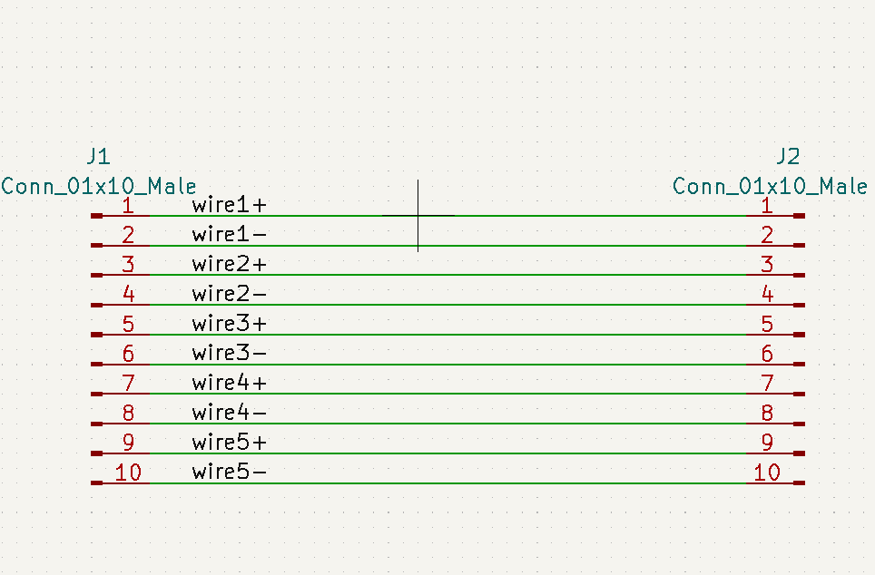
绘制原理图
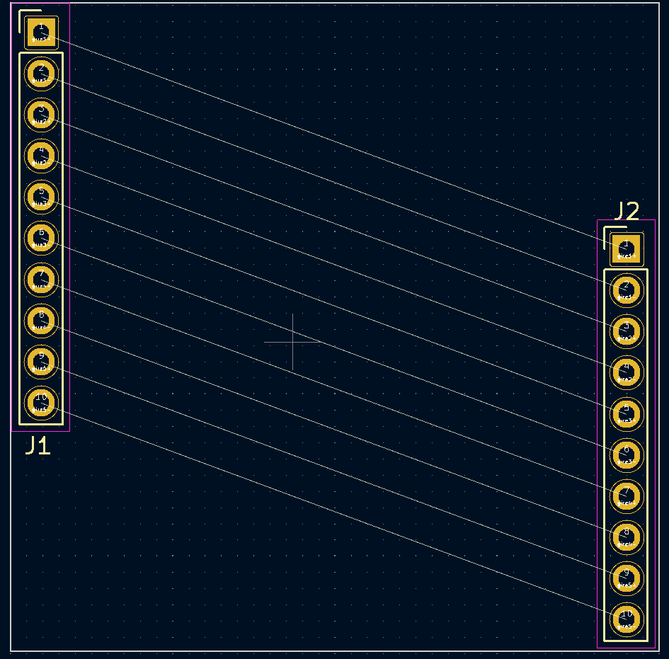
更新到PCB中
布局完成后我们就要绘制差分对了,我们正常布线的时候是一根一根线进行绘制的,差分对进行布线的时候是两根一起的,选择布线,差分对交互布线,或者直接按快捷键6进行绘制,如图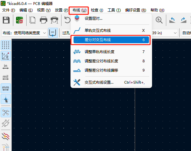
绘制差分对
我们选择需要绘制的点后单击就会出现两条走线,对应的另外一段需要连线的脚就会高亮起来如图: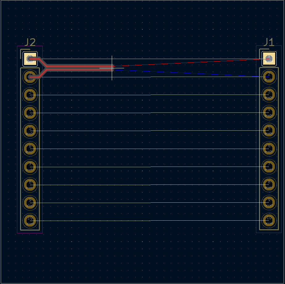
绘制差分对
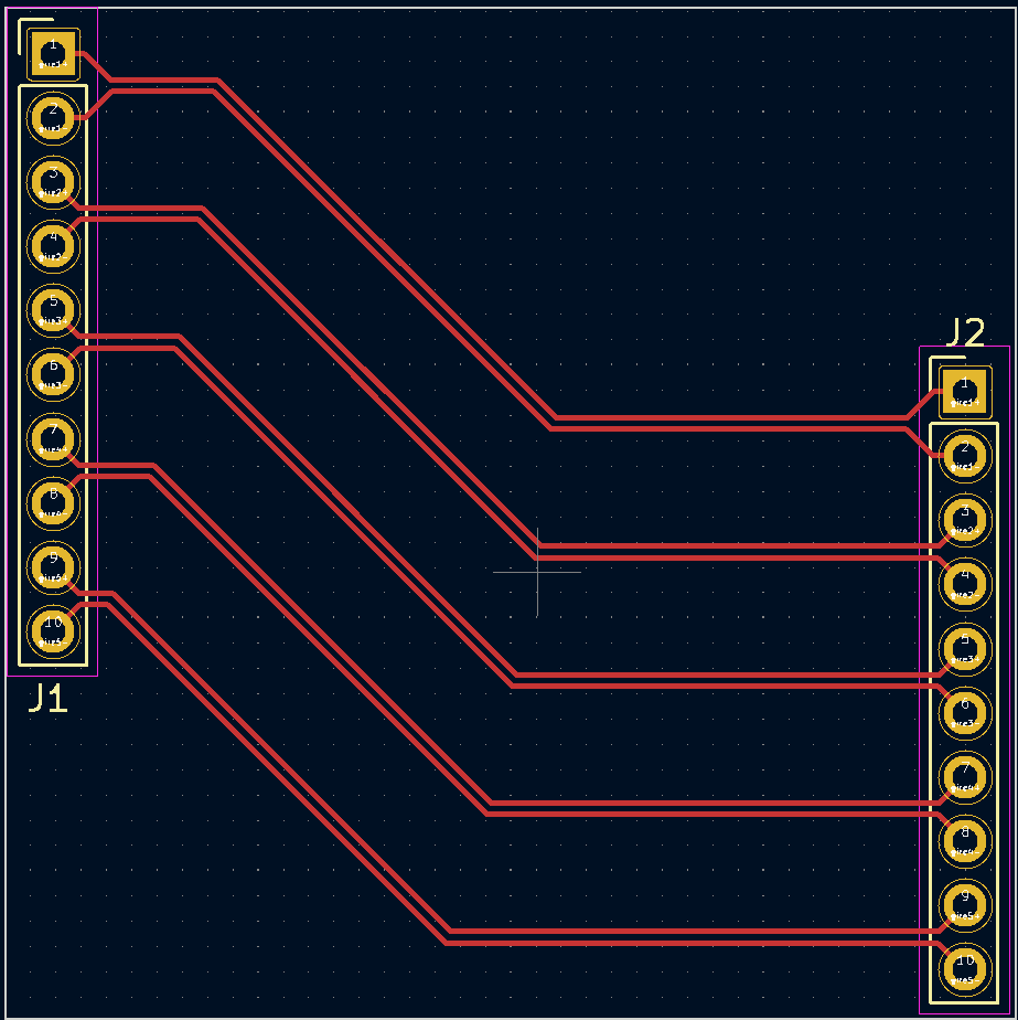
根据需求将线拖到另外一端的脚即可,中间可以调节查分线的走向,如图这样就绘制好了我们的差分对了如图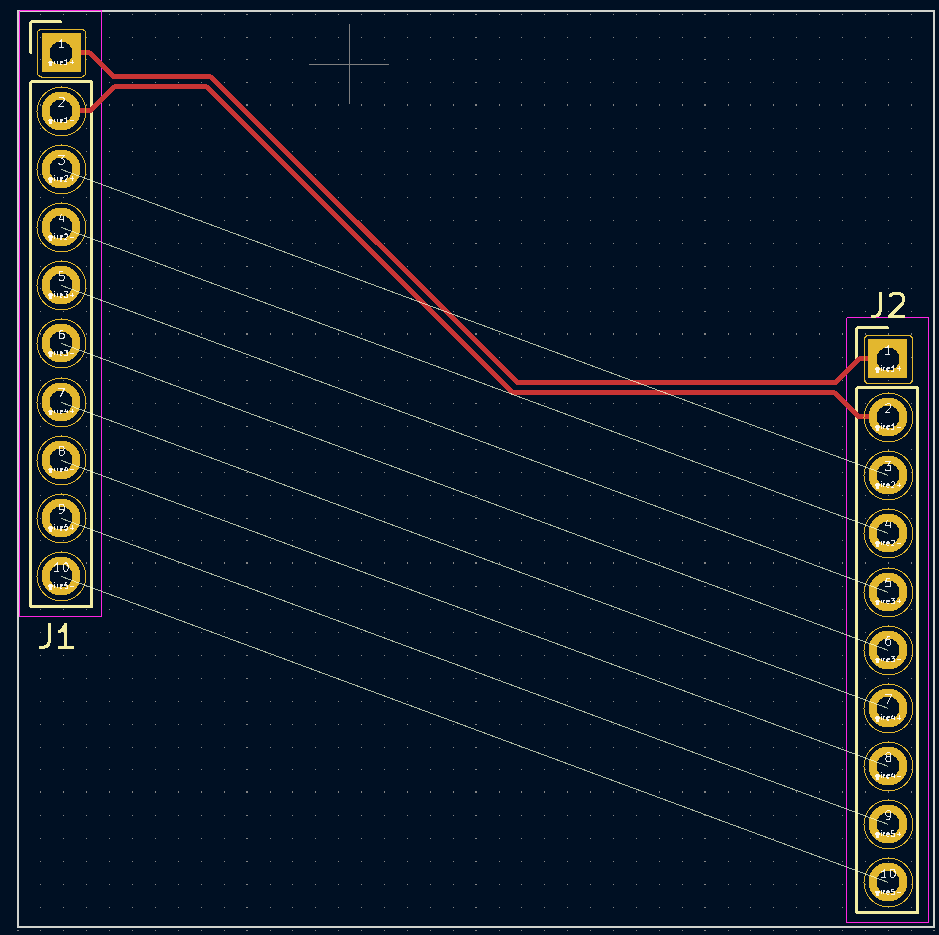
绘制差分对
绘制差分对
我们绘制原理图时都是以+、-结尾的,这边我把其中的一对修改成了普通的网络标签名,如图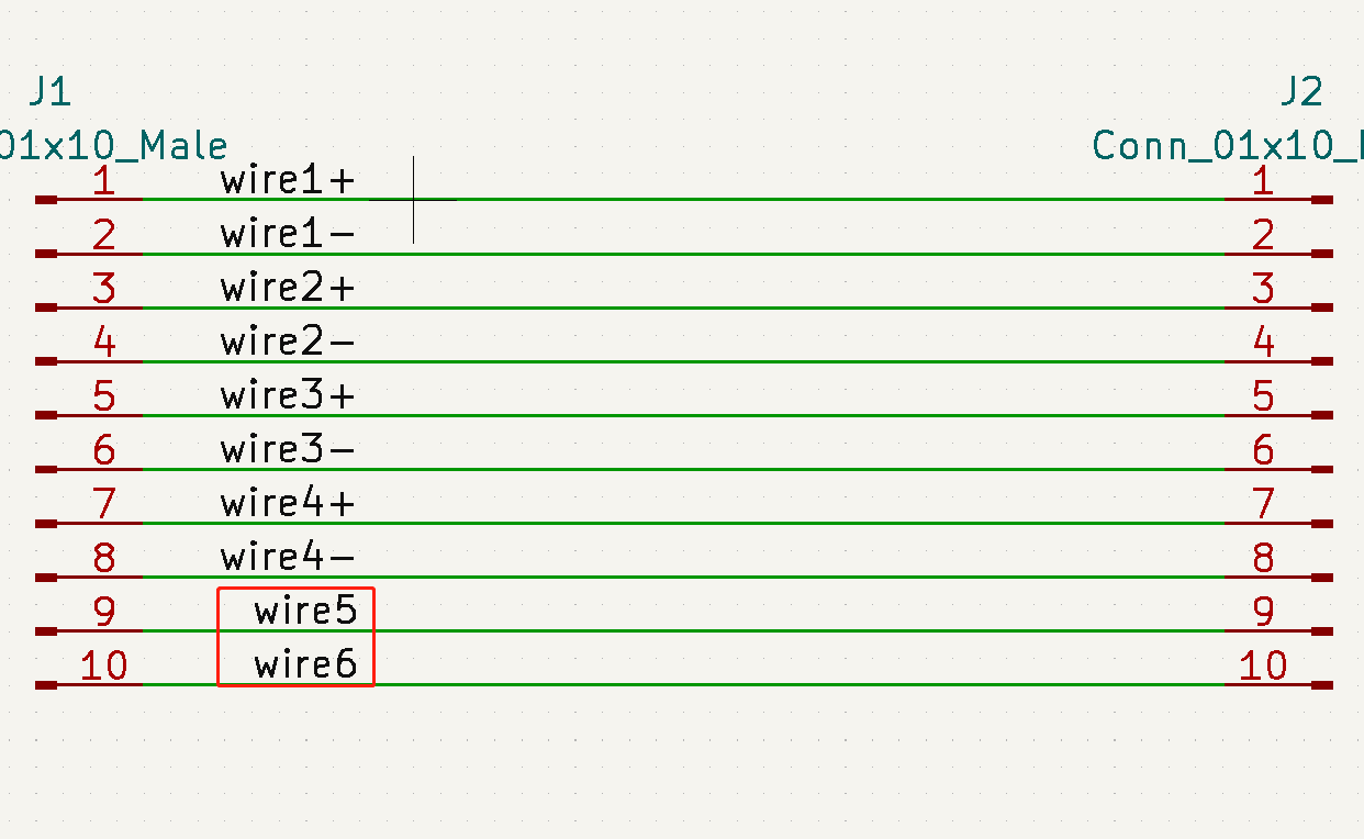
修改网络标签名
这个时候我们再使用差分对就行布线会出现什么情况呢,和刚才一样选择绘制差分对,点击需要绘制的脚,如果选择的不是差分对,此时会提示不能够布线识别到差分对如图: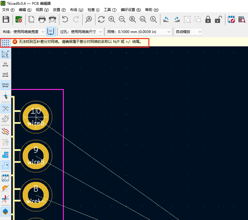
绘制差分对
所以我们再绘制前要把需要用差分对走线的网络都用网络标签标记好,这样再绘图时才会非常顺利。
这种是在布局非常合理且我们的走线非常顺畅的情况下绘制的差分对,如果差分对出现了交叉的情况,或者差分对与差分对之间出现了交叉的情况时又该怎么绘制呢,下面我们就来演示一下这种情况。
Differential pairs allow you to route two wires at the same time. This capability is useful in those cases where two adjacent wires are complementary and have to be treated as such. By routing the wires together, we can ensure that the travel time of the signal from origin to destination will be practically the same, as well as that they will receive an almost identical amount of interference. Differential pairs are important in applications such as audio, digital singling, data communications (RS-422, Ethernet etc). The technique helps to minimise electromagnetic interference and crosstalk. It also helps to minimise the noise that these wires emit to their environment.
KiCad, apart from allowing to draw differential pairs in the layout, also provides tools to configure them. You can set the total length of the pair, ensuring matching lengths of traces where that is important (like in high- speed memory applications). To enable the differential pair feature in Pcbnew, you need to label the participating nets in Eeschema with names that end with '+' and '-' or with 'N' and 'P'. Let’s have a look at a very simple example, depicted in Figure 44.1. Figure 44.1: The wires that belong to a pair have net names that end with '-' or ‘+’. In this example, I have two connectors, with wires connecting their pins. I have labeled the wires with net labels, and for each pair, the name of the label ends with either '+' or '-'. In place of '-' or '+' I could have used 'P' or 'N'.
When you export the netlist for this schematic and import it into Pcbnew, you will have a layout like the one in Figure 44.2. Figure 44.2: The unconnected layout view. You can route each net using individual routes, or use differential pair routing. To enable differential pair routing, choose this option from the Route menu (Figure 44.3). Figure 44.3: Enable differential pair routing. Then, click on one of the pads to begin drawing. You will see that you are now drawing two traces: one is connected to the pad you clicked on, and the other to its pair (Figure 44.4). Figure 44.4: Started drawing a differential pair. Click on the pad that is highlighted in the J2 connector to complete the drawing. The result is in Figure 44.5.
Figure 44.5: The first differential pair is routed. In the next example, try to route a differential pair but this time add vias, like in Figure 44.6. As you can see, by typing 'V' you create two vias, one for each trace member of the pair. Figure 44.6: The second differential pair is traced in the B.Cu with the help of vias. KiCad allows you to fine-tune the length of a trace. This allows you to control the signal propagation through the trace, precisely. Let’s try this out. Start by clicking on the 'Tune Track Length' option from the Route menu. Then, click on a member trace of one of the differential pairs that you want to tune the length for. This will give you information about the current length of that trace (Figure 44.7). In this example, the trace I clicked on is shorter than the target. Figure 44.7: The current length of this trace is 37.056 mm; the target is 40 mm. To configure the target length, right click on the trace and click on the 'Length Tuning Settings…' option. In the window that comes up, define the track length target. There are other options you can experiment with, that define the characteristics of the meanders that KiCad uses to adjust the trace length. I have changed my target length to 40 mm (Figure 44.8).
Figure 44.8: You can control the characteristics of differential per traces. To adjust a trace so that its length becomes equal to the target, click on a trace to select it and move your mouse to the direction where you want to meanders to appear. KiCad will keep you informed about the current length of the trace. When you reach the target, click to commit the changes. Figure 44.9: Adjusting the length of a differential trace. Repeat the same process for the rest of the differential traces. If the length adjustment is blocked by a via, continue on the other side of the via.
You can tune the length of both traces in a pair at the same time by selecting the 'Tune Differential Pair Length' option from the Route menu.
