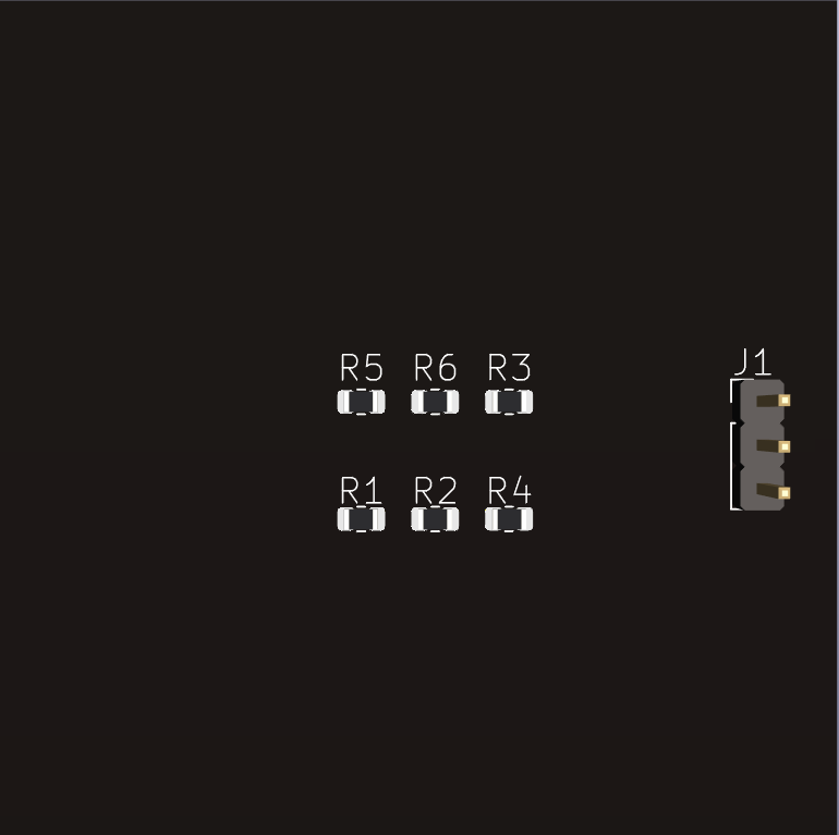
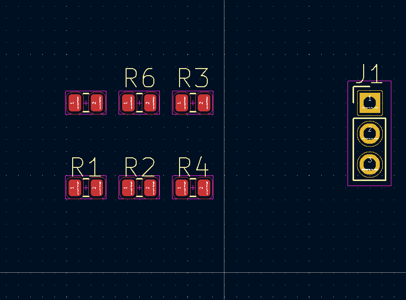
在PcbNew中批量调整文本和图形的属性
B站视频:
下面我就来演示一下另外一种批量修改丝印的方式,首先点击编辑-选择编辑文本与图形属性如图: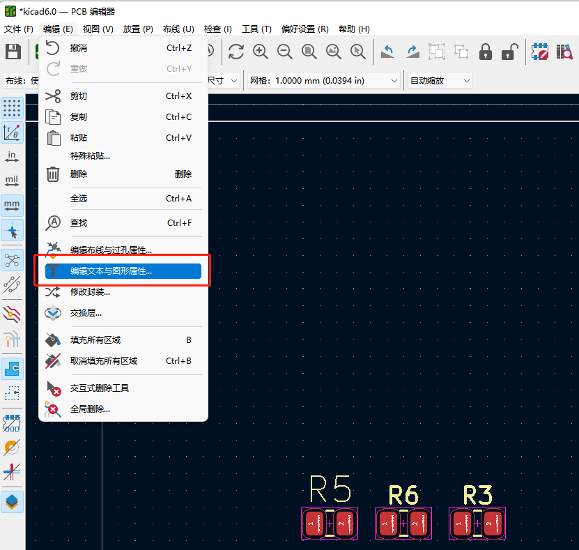
编辑文本与属性
进入编辑文本和图形属性框,这边因为我们修改的是位号,所以这边勾选位号,文本高度文本宽度都改成0.1,文本粗细改成0.1,其余不变如图: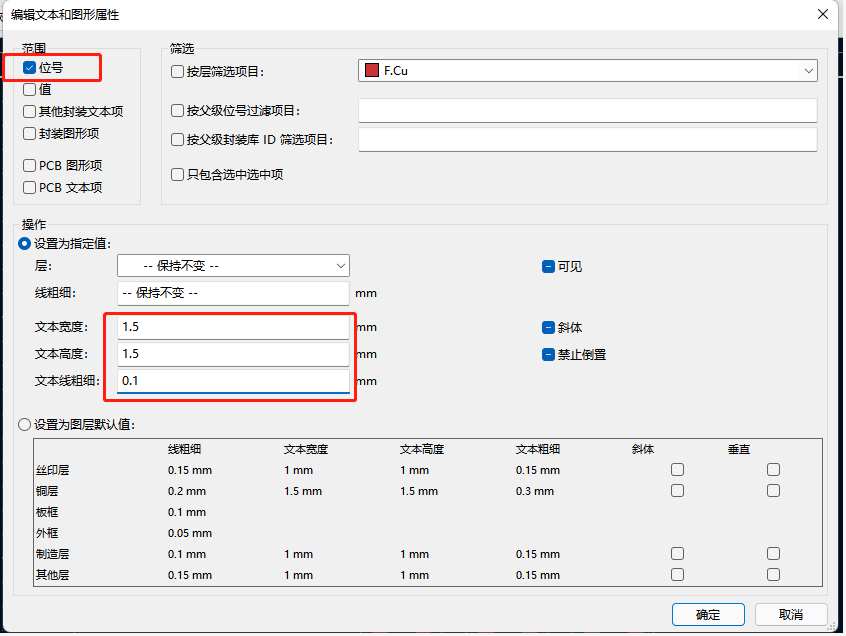
编辑文本与属性
编辑完成后点击确认我们可以看到所有位号丝印都改成了统一的大小如图: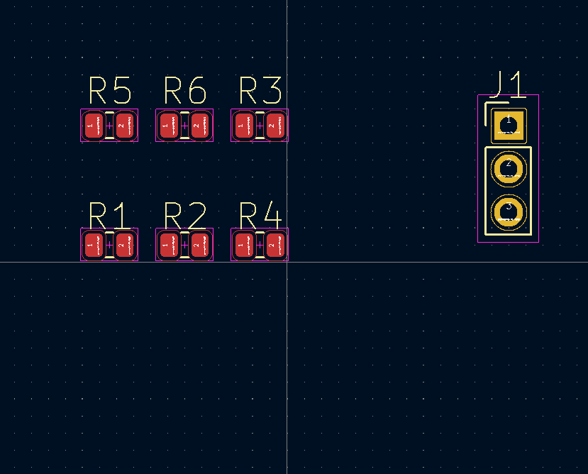
修改位号的丝印大小
查看3D模型
如果当我们器件布局比较紧密的时候,我们其实是可以不需要添加这些位号的,这时我们就可以就可以将这些位号进行隐藏,如果只想隐藏部分的位号的话我们就可以直接双击位号,弹出封装位号属性,显示的对话框取消勾选如图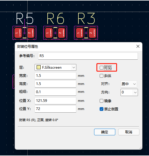
封装位号属性
位号隐藏
接下来我们再演示一下如何批量隐藏位号,打开刚才的编辑文本与图形属性框,我们操作的对象还是位号,所以还是选择位号,然后在层的这一栏中的可见前的选框取消勾选,其余不变,如图: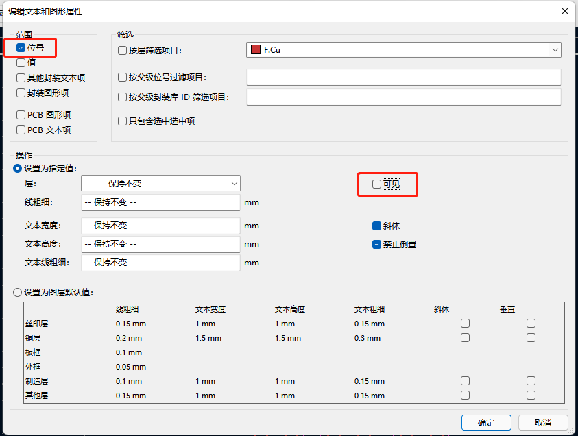
隐藏位号
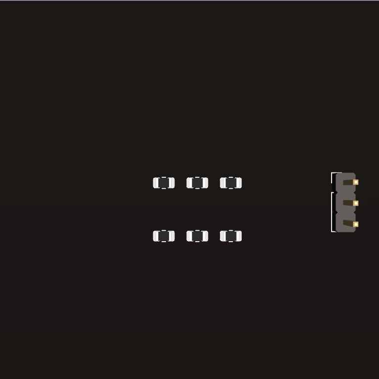
点击确认后可以发现所有的位号都被隐藏掉了,我们再看一下3D效果图如图: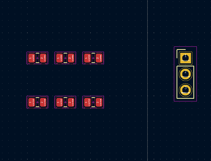
隐藏位号
查看3D模型
KiCad provides user interface tools to help you make multiple changes in a single step. For example, you can change all silkscreen layer text items to have a uniform height and width. You can also be specific in terms of scope, and change text attributes of all footprint values or reference text items at once. Apart from text properties, you can also change graphics, track and via properties in bulk. With the help of special filters, you can be very specific. For example, you can change the width of all power tracks on the top copper layer to a new value. The global change tool you will learn about in this recipe works in Pcbnew. In this recipe, you will learn how to change all footprint values text item properties so that they are uniform. To do this, I will use the breadboard power supply project, which is Project 1 in this book. To begin with, we have a PCB that looks like the one in Figure 59.1. Figure 59.1: The starting point of this recipe: the arrows show the text items that I will modify their attributes in bulk. I only show a segment of the full PCB to make it easier to distinguish the text items that I will be changing the attributes of. Those are indicated by the red arrows. I would like to reduce the size (height and width) of those items, just slightly, to make it easier to fit in the available space on this PCB. What these items have in common, is that they are independent PCB text items. I created them using the text tool in Pcbnew, and are not attached to a footprint. Of course, it is possible to make bulk changes to any other text item on the board, as long as you know what type of item it is (such as “footprint values” or “footprint reference” etc.) so that you can target them with the appropriate filter. Let’s continue with the independent PCB text items. Currently the size of each character in these items is 1mm x 1mm (width x height) with a thickness of 0.25mm. You can verify this by getting the item properties (hover you mouse over the item, and type “E”). Figure 59.2: Currently, the text item character size is 1mm x 1mm. Let’s change these dimensions to 0.8mm x 0.8mm, and the thickness to 0.2mm. Click on Edit, Edit Text & Graphic Properties… Figure 59.3: Bring up the Edit Text properties window This will bring up the edit window, as in the screenshot in .
Figure 59.4: This edit window gives you a lot of flexibility to change text item properties. This edit window gives you a lot of flexibility as to what is it that you want to change, and what change to introduce. Under “scope” and “Filters” you can select the kind of text or graphic item that you want to change. To keep this example simple, I have chosen to change independent PCB text items, and that is why I have clicked on this specific checkbox. Note that these are checkboxes, not radio buttons, so you can choose multiple kinds of items and have changes applied on all of them. Under “Filters”, you can choose text of graphics items based on the layer that they exist, or a parent footprint reference or identifier. So, for example, you can choose all text items that belong to the LED footprints, etc. Once you have selected the kind of text or graphic item you want to change, go to the “Action” group to provide the details of the changes. In this example, again, lets keep it simple. I simply want to make the text smaller, so specify text width and height to 0.8mm. I also checked the “Visible” and “Keep upright” boxes, and unchecked “Italic”. I can also set my chosen text items to preset values, listed in the “Set to layer default values” box. For any values that you want to keep unchanged, leave the “…” in the respective field. Click OK to accept the changes. The result is Figure … Figure 59.5: The text items marked with the red arrow have the new attributes applied. Compare the “before” and “after” images of the PCB, and you will notice that the text items marked with the red arrow are slightly smaller then the originals. It only took a single interaction with a dialogue box to make this change, which affected multiple text items. You can use the exact same technic to bulk-change the attributes of graphics (like lines and circles), but also those of vias and traces. For example, try this little experiment. In this board, the power traces in the top copper layer is 0.3mm. Can you change the thickness of all top layer power traces to 0.35mm? (Hint: use the “Edit Text & Graphics Properties” window).
