**这是本文档旧的修订版!**
I2C是一种简单地连接多个芯片的总线方式,尤其是在FPGAs/CPLDs中.

概述
I2C总线特性
- Uses only 2 wires (named “SDA” and “SCL”) in addition to power and ground
- Can support over 100 devices on the same bus (each device on the bus has an address to be individually accessible)
- Multi-master (for example, two CPUs can easily share the same I2C devices)
- Industry standard (developed by Philips, adopted by many other manufacturers)
- Used everywhere (TVs, PCs…)
但是:
- Relatively slow (100Kbps base speed, with extensions up to 3.4Mbps)
- Not plug-and-play
工作原理
An I2C bus needs at a minimum an I2C master and an I2C slave. The I2C master is a transaction (a master can write-to or read-from a slave). The I2C slave is a transaction recipient (a slave can be written-to or read-from a master).
I2C波型
Here's how it looks on the bus. This a write to an EEPROM at address 0x51, with 2 data bytes 0x50 and 0x0F.
An I2C transaction begins with a “start” condition, followed by the address of the device we wish to speak to, a bit to indicate if we want to read or write, the data written or read, and finally a “stop”. There are other details, like the need to have an “acknowledge” bit after each byte transmitted… see the waveform above, and the project's links.
I2C从模式示例1
在FPGA或CPLD中有两种方式创建一个I2C slave
- 直接使用你FPGA/CPLD中的SCL信号线作为时钟信号
- 使用更快的时钟信号过取样你的SDA和SCL信号
第一种方法设计比较紧凑,但不如第二种方法可靠。
I2C slave示例1: 采用方法1进行IO扩展 - SCL在FPGA/CPLD中作为时钟信号
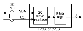
Here's a view of our IO extender.
The I2C slave module is connected to a small 8-bits memory that can be read and written from the I2C bus. The 8-bits are also exported outside the FPGA/CPLD. That creates an I2C IO extender.
First the module declaration. module I2CslaveWith8bitsIO(SDA, SCL, IOout); inout SDA; input SCL; output [7:0] IOout; Then the 7-bits address that we want for our I2C slave. parameter I2CADR = 7'h27; Then the start and stop conditions detection logic. That's the “black magic” part of this design… We use two wires with a combinatorial loop to detect the start and stop conditions … making sure these two wires don't get optimized away wire SDAshadow /* synthesis keep = 1 /; wire startorstop / synthesis keep = 1 */; assign SDAshadow = (~SCL | startorstop) ? SDA : SDAshadow; assign startorstop = ~SCL ? 1'b0 : (SDA ^ SDA_shadow);
reg incycle; always @(negedge SCL or posedge startorstop) if(startorstop) incycle ⇐ 1'b0; else if(~SDA) incycle ⇐ 1'b1; Now we are ready to count the I2C bits coming in reg [3:0] bitcnt; counts the I2C bits from 7 downto 0, plus an ACK bit wire bitDATA = ~bitcnt[3]; the DATA bits are the first 8 bits sent wire bitACK = bitcnt[3]; the ACK bit is the 9th bit sent reg data_phase; always @(negedge SCL or negedge incycle) if(~incycle) begin bitcnt ⇐ 4'h7; the bit 7 is received first dataphase ⇐ 0; end else begin if(bitACK) begin bitcnt ⇐ 4'h7; dataphase ⇐ 1; end else bitcnt ⇐ bitcnt - 4'h1; end and detect if the I2C address matches our own wire adrphase = ~dataphase; reg adrmatch, opread, gotACK; sample SDA on posedge since the I2C spec specifies as low as 0µs hold-time on negedge reg SDAr; always @(posedge SCL) SDAr⇐SDA; reg [7:0] mem; wire opwrite = ~opread; always @(negedge SCL or negedge incycle) if(~incycle) begin gotACK ⇐ 0; adrmatch ⇐ 1; opread ⇐ 0; end else begin if(adrphase & bitcnt==7 & SDAr!=I2CADR[6]) adrmatch⇐0; if(adrphase & bitcnt==6 & SDAr!=I2CADR[5]) adrmatch⇐0; if(adrphase & bitcnt==5 & SDAr!=I2CADR[4]) adrmatch⇐0; if(adrphase & bitcnt==4 & SDAr!=I2CADR[3]) adrmatch⇐0; if(adrphase & bitcnt==3 & SDAr!=I2CADR[2]) adrmatch⇐0; if(adrphase & bitcnt==2 & SDAr!=I2CADR[1]) adrmatch⇐0; if(adrphase & bitcnt==1 & SDAr!=I2CADR[0]) adrmatch⇐0; if(adrphase & bitcnt==0) opread ⇐ SDAr; we monitor the ACK to be able to free the bus when the master doesn't ACK during a read operation if(bitACK) got_ACK ⇐ ~SDAr; if(adrmatch & bitDATA & dataphase & opwrite) mem[bitcnt] ⇐ SDAr; memory write end and drive the SDA line when necessary. wire membitlow = ~mem[bitcnt[2:0]]; wire SDAassertlow = adrmatch & bitDATA & dataphase & opread & membitlow & gotACK; wire SDAassertACK = adrmatch & bitACK & (adrphase | opwrite); wire SDAlow = SDAassertlow | SDAassertACK; assign SDA = SDAlow ? 1'b0 : 1'bz; assign IOout = mem; endmodule What's the result? The code has been tested in multiple devices (Xilinx FPGA, Altera FPGA/CPLD), with an hard-macro I2C master (Dragon board). The complete code is available here. This code has two drawbacks: The SCL signal is used as a clock in the FPGA/CPLD. The use of a Schmitt trigger on the SCL input pin is strongly recommended to avoid erratic behavior (without Schmitt trigger, any noise or ringing on the SCL line may introduce extra clock cycles, which would break the functionality). The start and stop conditions detection logic uses a combinatorial feedback loop, which is not a recommended practice. Same thing on the “incycle” signal that is used as asynchronous reset by the rest of the logic. These are the price to pay to avoid using an oversampling clock. If you can live with these drawbacks, you get a very compact I2C slave design. Otherwise, use an external clock to oversample SDA and SCL (method 2). This way, glitches can be filtered out using digital filters, and the start and stop condition detected easily (at the price of a more complex design). External contributions Contributed by an fpga4fun readers… I2C simulation in Verilog I2C slave in VHDL ====== I2C从模式示例2 ====== ====== An example of I2C master ====== ====== A logic analyzer, to capture live I2C transaction and spy on the bus ====== …not ready yet ====== 资源链接 ====== * I2C规范. * Philips多方面深度讨论I2C的应用指南 * I2C常见问题 * [http://www.totalphase.com/support/kb/10040/|关于I2C和SMBus区别的文章]
