**这是本文档旧的修订版!**
扫描二维码,关注微信公众号“电子森林”,可以在手机上查看本网站的所有文章
SPI - 同步、全双工的串行外设接口
SPI(Serial Peripheral Interface - 同步外设接口)总线是一种用于短距离通信(主要是嵌入式系统中)的同步串行通信接口规范,虽然没有正式的国际标准,但这种接口协议由Motorola发明迄今经过很多厂商的支持,已经成了一种事实标准,被广泛用于各种MCU处理器中,同传感器,串行ADC、DAC、存储器、SD卡以及LCD等进行数据连接。
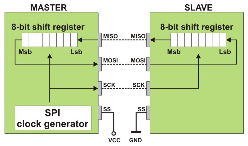
主、从器件之间的连接及数据传输方式
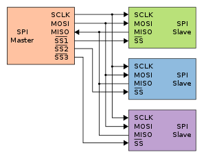
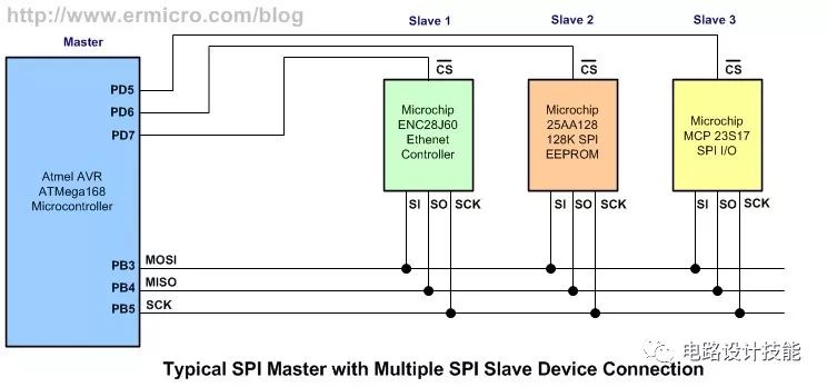
多个SPI设备可以通过全双工的模式同单一的Master以主、从结构进行通信。主、设备发起读、写,多个从设备通过独立的片选信号(SS - Slave Select)被寻址。
SPI总线:单主多从连接
有时SPI也被称为四线串行总线,主要是与3线、2线、1线串行总线进行区分,虽然SPI可以准确地描述为一个同步串行接口,但它与同步串行接口(SSI)协议还是不同的,SSI同样也是一种4线同步串行通信协议,但SSI采用的是差分信号,且只提供了一个简单的通信信道。

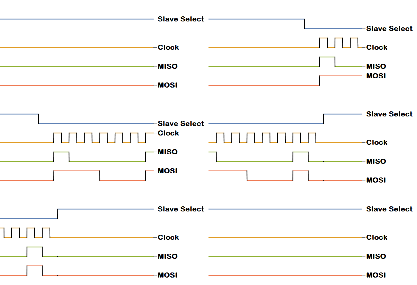
动画1显示数据从器件A移出到器件B,从器件B移出到器件A.
SPI的技术实现
接口信号
SPI总线定义了4个逻辑信号:
- SCLK: 串行时钟(由主设备输出).
- MOSI: 主输出、从输入(由主设备输出).
- MISO: 主输入、从输出(由从设备输出).
- SS: 从设备选中(低有效, 由主设备输出).
SPI端口管脚的名字也有其它的叫法,不同的芯片公司叫法不同,比如:
- 串行输出: SCLK : SCK, CLK.
- 主输出 –> 从输入: MOSI : SIMO, SDI(对于“从”设备), DI, DIN, SI, MTST.
- 主输入 ←- 从输出: –> MISO : SOMI, SDO (对于“从”设备), DO, DOUT, SO, MRSR.
- 从选择: SS : nCS, CS, CSB, CSN, EN, nSS, STE, SYNC.
动画2显示了通过一个虚拟的4通道示波器捕捉的两个器件之间SPI的转换
工作模式
SPI总线可以工作在一个主设备/一个或多个从设备的模式。 如果只有一个从设备,SS管脚可以直接接地(从设备允许的话),有些从设备需要片选信号的下降沿来启动传输,一个例子就是美信公司的串行ADC MAX1242,通过一个高电平到低电平的转换标记传输的起始。如果有多个从设备,每个从设备需要一个独立的SS信号连接到主设备。
多数从设备的输出是三态的,当该从设备没有被选中的时候它们的MISO信号就为高阻(逻辑上断开连接)。不具有三态输出的器件是不能同其它器件共享SPI总线部分的,只能是一个从设备跟主设备相连。
SPI的时钟采样
通过多个从片选信号(SSN)配置
在标准的SPI配置中,主设备可以通过使能相应的从设备,即通过将相应设备的从选择线(SSN或SS)设置为逻辑低电平,通过共享的公共数据线将数据写入各个从设备或由各个从设备中读取数据。 应注意不要同时使能多个从设备,因为返回到主设备的数据将在MISO线路之间的驱动器上产生竞争导致无法进行数据的判读。在某些应用中不需要将数据返回给主设备,在这种情况下,如果主设备想要将相同的数据发送到多个从设备,则可以同时寻址多个从设备。
在多从设备选择配置中,每个从设备都需要来自主设备的唯一从设备选择线(SS、SSN或CSn)。如果主设备没有足够的I/O引脚用于所需数量的从设备,则使用解码/解复用器(例如74HC(T)238(3到8线)来实现I/O扩展)。
菊花链配置
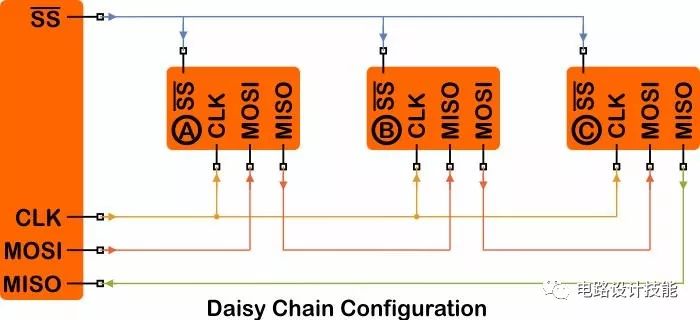
在这种配置中,数据从一个设备移动到下一个设备, 最终的从设备可以将数据返回给主设备(给FPGA编程的JTAG在给多个器件编程的时候也常用这种方式)。
在菊花链配置中,所有从设备共享一条公共的从选择线(SS)。 数据从主设备传输到第一个从设备,然后从第一个从设备传输到第二个从设备,依此下去,数据沿着线路级联,直到系列中的最后一个从设备,最后的一个从设备使用其MISO线路将数据传送到主设备。
这种配置非常适合于主设备的信号引脚有限的场景。
4种传输模式
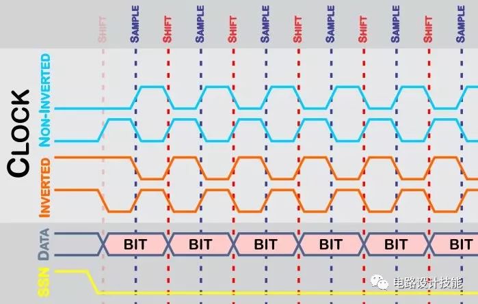
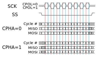
每次数据传输都是先将SSN(有的器件命名为SS,从选择线)被驱动为逻辑低电平时开始。由时钟的极性(CPOL)和相位(CPHA)构成了4种不同的数据传输模式(0,1,2,3),分别对应四种可能的时钟配置。
- CPOL: 时钟的极性,它控制着时钟信号的初始逻辑状态。
- CPHA: 时钟相位,它控制了数据转换和时钟转换之间的关系。
具有非反相时钟极性(即,当从器件选择转换为逻辑低时,时钟处于逻辑低电平):
- 模式0:配置时钟相位使得数据在时钟脉冲的上升沿采样,并在时钟脉冲的下降沿移出。 这对应于上图中的第一个蓝色时钟轨迹。 请注意,数据必须在时钟的第一个上升沿之前可用。
- 模式1:配置时钟相位使得数据在时钟脉冲的下降沿采样,并在时钟脉冲的上升沿移出。 这对应于上图中的第二个蓝色时钟轨迹。
使用反相时钟极性(即,当从器件选择转换为逻辑低时,时钟处于逻辑高电平):
- 模式2:配置时钟相位,使得数据在时钟脉冲的下降沿采样,并在时钟脉冲的上升沿移出。 这对应于上图中的第一个橙色时钟轨迹。 请注意,数据必须在时钟的第一个下降沿之前可用。
- 模式3:配置时钟相位,使得数据在时钟脉冲的上升沿采样,并在时钟脉冲的下降沿移出。 这对应于上图中的第二个橙色时钟轨迹。
由于主设备一般为可以编程各种模式的控制器/处理器或者可以灵活编程的FPGA,因此在使用SPI连接的时候要认真阅读自己选用的从设备的工作模式,以便在时序上满足传输的要求。
SPI数据传输的主设备端代码示例
以下是一段主设备工作于CPOL=0、CPHA=0模式时的数据传输的代码,每次传输为8位,此示例采用C语言。由于工作于CPOL=0, 在片选被选中之前要把时钟拉低,片选信号必须使能,也就是说在数据传输之前要将外设的片选信号电平变低,并在传输结束以后不再“使能”。 多数的外设允许或需要在片选信号选中以后进行多次传输,次子程序也许需要被多次调用。
/*
 * Simultaneously transmit and receive a byte on the SPI.
 *
 * Polarity and phase are assumed to be both 0, i.e.:
 *   - input data is captured on rising edge of SCLK.
 *   - output data is propagated on falling edge of SCLK.
 *
 * Returns the received byte.
 */
uint8_t SPI_transfer_byte(uint8_t byte_out)
{
    uint8_t byte_in = 0;
    uint8_t bit;

    for (bit = 0x80; bit; bit >>= 1) {
        /* Shift-out a bit to the MOSI line */
        write_MOSI((byte_out & bit) ? HIGH : LOW);

        /* Delay for at least the peer's setup time */
        delay(SPI_SCLK_LOW_TIME);

        /* Pull the clock line high */
        write_SCLK(HIGH);

        /* Shift-in a bit from the MISO line */
        if (read_MISO() == HIGH)
            byte_in |= bit;

        /* Delay for at least the peer's hold time */
        delay(SPI_SCLK_HIGH_TIME);

        /* Pull the clock line low */
        write_SCLK(LOW);
    }

    return byte_in;
}
SPI的优点和缺点
优点
- 支持全双工通信
- 推挽驱动(跟漏极开路正相反)提供了比较好的信号完整性和较高的速度
- 比I²C或SMBus吞吐率更高
- 协议非常灵活支持“位”传输
- 不仅限于8-bit一个字节的传输
- 可任意选择的信息大小、内容、以及用途
- 异常简单的硬件接口:
- 一般来讲比I²C或SMBus需要的功耗更低,因为需要更少的电路(包括上拉电阻)
- 没有仲裁机制或相关的失效模式
- “从设备”采用的是“主设备”的时钟,不需要精确的晶振
- “从设备”不需要一个单独的地址 — 这点不像I²C或GPIB或SCSI
- 不需要收/发器
- 在一个IC上只用了4个管脚, 板上走线和布局连接都比并行接口简单很多
- 每个设备最多只有一个单独的总线信号(片选);其它的都是共享的
- 信号都是单方向的,非常容易进行电流隔离
- 对于时钟的速度没有上限,有进一步提高速度的潜力
缺点
- 相比于I²C总线需要更多的管脚, 即便是只用到3根线的情况下
- 没有寻址机制,在共享的总线连接时需要通过片选信号支持多个设备的访问
- 在从设备侧没有硬件流控机制(主设备一侧可以通过延迟到下一个时钟沿以降低传输的速率)
- 从设备无法进行硬件“应答”(主设备传送的信息无法确定传递到哪里,是否传递成功)
- 一般只支持一个主设备(取决于设备的硬件构成)
- 没有查错机制
- 没有一个正式的标准规范,无法验证一致性
- 相对于RS-232, RS-485, 或CAN-总线,只能近距离传输
- 存在很多的变种,很难能够找到开发工具(例如主适配卡)支持这所有的变种
- SPI不支持热交换(动态地增加一个节点).
- 如果想使用“中断”,只有通过SPI信号以外的其它信号线,或者采用类似USB1.1或2.0中的周期性查询的欺骗方式
- 有一些变种比如多路I/O SPI和下面定义的三线串行总线都是半双工的
应用
The board real estate savings compared to a parallel I/O bus are significant, and have earned SPI a solid role in embedded systems. That is true for most system-on-a-chip processors, both with higher end 32-bit processors such as those using ARM, MIPS, or PowerPC and with other microcontrollers such as the AVR, PIC, and MSP430. These chips usually include SPI controllers capable of running in either master or slave mode. In-system programmable AVR controllers (including blank ones) can be programmed using an SPI interface.
Chip or FPGA based designs sometimes use SPI to communicate between internal components; on-chip real estate can be as costly as its on-board cousin.
The full-duplex capability makes SPI very simple and efficient for single master/single slave applications. Some devices use the full-duplex mode to implement an efficient, swift data stream for applications such as digital audio, digital signal processing, or telecommunications channels, but most off-the-shelf chips stick to half-duplex request/response protocols.
SPI is used to talk to a variety of peripherals, such as
- Sensors: temperature, pressure, ADC, touchscreens, video game controllers
- Control devices: audio codecs, digital potentiometers, DAC
- Camera lenses: Canon EF lens mount
- Communications: Ethernet, USB, USART, CAN, IEEE 802.15.4, IEEE 802.11, handheld video games
- Memory: flash and EEPROM
- Real-time clocks
- LCD, sometimes even for managing image data
- Any MMC or SD card (including SDIO variant[5])
For high performance systems, FPGAs sometimes use SPI to interface as a slave to a host, as a master to sensors, or for flash memory used to bootstrap if they are SRAM-based.
Although there are some similarities between the SPI bus and the JTAG (IEEE 1149.1-2013) protocol, They are not interchangeable. The SPI bus is intended for high speed, on board initialization of device peripherals, while the JTAG protocol is intended to provide reliable test access to the I/O pins from an off board controller with less precise signal delay and skew parameters. While not strictly a level sensitive interface, the JTAG protocol supports the recovery of both setup and hold violations between JTAG devices by reducing the clock rate or changing the clock's duty cycles. Consequently, the JTAG interface is not intended to support extremely high data rates.
SGPIO is essentially another (incompatible) application stack for SPI designed for particular backplane management activities.[citation needed] SGPIO uses 3-bit messages.
开发工具
When developing or troubleshooting systems using SPI, visibility at the level of hardware signals can be important.
主适配卡
There are a number of USB hardware solutions to provide computers, running Linux, Mac, or Windows, SPI master and/or slave capabilities. Many of them also provide scripting and/or programming capabilities (Visual Basic, C/C++, VHDL etc.).
An SPI host adapter lets the user play the role of a master on an SPI bus directly from PC. They are used for embedded systems, chips (FPGA/ASIC/SoC) and peripheral testing, programming and debugging.
The key parameters of SPI adapters are: the maximum supported frequency for the serial interface, command-to-command latency and the maximum length for SPI commands. It is possible to find SPI adapters on the market today that support up to 100 MHz serial interfaces, with virtually unlimited access length.
SPI protocol being a de facto standard, some SPI host adapters also have the ability of supporting other protocols beyond the traditional 4-wires SPI (for example, support of quad-SPI protocol or other custom serial protocol that derive from SPI[8]).
Examples of SPI adapters (manufacturers in alphabetical order):
| 生产商 | SPI Host适配卡 | Host总线 | 支持的总线协议 | 最高频率 |
|---|---|---|---|---|
| Byte Paradigm | SPI Storm | USB | SPI, dual/quad, custom | 100 MHz |
| Corelis | BusPro-S | USB | SPI, dual/quad | 60 MHz |
| HydraBus | HydraBus-HydraFW | USB | SPI | 42 MHz |
| Microchip | MCP2210 Kit | USB | SPI | 12 MHz |
| National Instruments | USB-8452 | USB | I²C, SPI | 50 MHz |
| Total Phase | Cheetah SPI Host Adapter | USB | SPI | 40 MHz |
| Total Phase | Promira Serial Platform | USB, Ethernet | I²C, SPI, single/dual/quad, and eSPI | 80 MHz |
| Dangerous Prototypes | Bus Pirate | USB | 1-Wire, I2C, SPI, JTAG*, Asynchronous serial, Scriptable binary bitbang, UART | varies |
协议分析仪
SPI protocol analyzers are tools which sample an SPI bus and decode the electrical signals to provide a higher-level view of the data being transmitted on a specific bus.
Examples of SPI protocol analyzers (manufacturers in alphabetical order):
| Manufacturer | Analyser model | Host bus | Bus protocol support | Max sample rate | Extras |
|---|---|---|---|---|---|
| Saleae Logic Pro 16 | USB | SPI, I2C, serial, custom | 500 Mega-samples/second | Analog (50 Mega-samples/second) | |
| TechTools | DigiView Logic Analyzers | USB | SPI, I2C, CAN, Async, Sync, I2S, State, Custom | 500 Mega-samples/second | Extendable with custom plugins |
| Total Phase | Beagle I2C/SPI Protocol Analyzer | USB | SPI, I2C, MDIO | 50 Mega-samples/second | |
| Total Phase | Promira Serial Platform | USB, Ethernet | eSPI |
示波器
Every major oscilloscope vendor offers oscilloscope-based triggering and protocol decoding for SPI. Most support 2-, 3-, and 4-wire SPI. The triggering and decoding capability is typically offered as an optional extra. SPI signals can be accessed via analog oscilloscope channels or with digital MSO channels.[9]
逻辑分析仪
When developing and/or troubleshooting the SPI bus, examination of hardware signals can be very important. Logic analyzers are tools which collect, analyze, decode, and store signals so people can view the high-speed waveforms at their leisure. Logic analyzers display time-stamps of each signal level change, which can help find protocol problems. Most logic analyzers have the capability to decode bus signals into high-level protocol data and show ASCII data.
相关术语
Intelligent SPI controllers
A queued serial peripheral interface (QSPI) is a type of SPI controller that uses a data queue to transfer data across the SPI bus.[10] It has a wrap-around mode allowing continuous transfers to and from the queue with only intermittent attention from the CPU. Consequently, the peripherals appear to the CPU as memory-mapped parallel devices. This feature is useful in applications such as control of an A/D converter. Other programmable features in QSPI are chip selects and transfer length/delay.
SPI controllers from different vendors support different feature sets; such DMA queues are not uncommon, although they may be associated with separate DMA engines rather than the SPI controller itself, such as used by multichannel buffered serial port (MCBSP).[11] Most SPI master controllers integrate support for up to four chip selects,[12] although some require chip selects to be managed separately through GPIO lines.
Microwire
Microwire, often spelled μWire, is essentially a predecessor of SPI and a trademark of National Semiconductor. It's a strict subset of SPI: half-duplex, and using SPI mode 0. Microwire chips tend to need slower clock rates than newer SPI versions; perhaps 2 MHz vs. 20 MHz. Some Microwire chips also support a three-wire mode, which fits neatly with the restriction to half-duplex.
Microwire/Plus
Microwire/Plus is an enhancement of Microwire and features full-duplex communication and support for SPI modes 0 and 1. There was no specified improvement in serial clock speed.
Three-wire serial buses
As mentioned, one variant of SPI uses single bidirectional data line (slave out/slave in, called SISO) instead of two unidirectional ones (MOSI and MISO). This variant is restricted to a half duplex mode. It tends to be used for lower performance parts, such as small EEPROMs used only during system startup and certain sensors, and Microwire. Few SPI master controllers support this mode; although it can often be easily bit-banged in software.
Multi I/O SPI
As opposed to three-wire serial buses, multi I/O SPI uses multiple parallel data lines (e.g., IO0 to IO3) to increase throughput. Dual I/O SPI using two data lines has comparable throughput to fast single I/O (MISO/MOSI). Quad I/O SPI using four data lines has approximately double the throughput.[15] Multi I/O SPI devices tend to be half duplex similar to three-wire devices to avoid adding too many pins. These serial memory devices combine the advantage of more speed with reduced pin count as compared to parallel memory.
mSPI
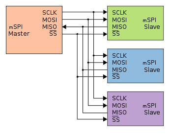 Typical mSPI bus: master and three independent slaves
mSPI (mini-SPI) is a modification initially developed by Dimitech for their programmable modules. Unlike the standard SPI, four signal lines are always required no matter of the number of slave devices. Its overall simplicity allows the use of standard SPI controllers with a very thin software layer.
All slave devices share the same SS (Slave Select; active low) line, along with the other three SPI signals: SCLK, MOSI and MISO. Additionally all slave devices normally have their MISO line disconnected from the bus in a high impedance state. As in the standard SPI, begin of transmission is marked by the activation of the SS line low and the end is marked by its return to high. mSPI requires the bus master to issue a “slave address” (typically 8 bits) as mandatory first word in every transmission. Since all slave devices share the same SS line, the address word will be received by all of them at the same time. From that point further, only the device with the specified address will connect its MISO line to the bus and start communicating, while all other slave devices will ignore any data and wait for a new start of transmission and address. mSPI solves some of the basic disadvantages of the standard SPI at the expense of a slight decrease in the overall communication speed due to the initial addressing.
Intel Enhanced Serial Peripheral Interface Bus
Intel has developed a successor to its Low Pin Count (LPC) bus that it calls the Enhanced Serial Peripheral Interface Bus, or eSPI for short. Intel aims to allow the reduction in the number of pins required on motherboards compared to systems using LPC, have more available throughput than LPC, reduce the working voltage to 1.8 volts to facilitate smaller chip manufacturing processes, allow eSPI peripherals to share SPI flash devices with the host (the LPC bus did not allow firmware hubs to be used by LPC peripherals), tunnel previous out-of-band pins through the eSPI bus, and allow system designers to trade off cost and performance.[16]
The eSPI bus can either be shared with SPI devices to save pins or be separate from the SPI bus to allow more performance, especially when eSPI devices need to use SPI flash devices.
This proposed standard defines an Alert# signal that is used by an eSPI slave to request service from the master. In a performance-oriented design or a design with only one eSPI slave, each eSPI slave will have its Alert# pin connected to an Alert# pin on the eSPI master that is dedicated to each slave, allowing the eSPI master to grant low-latency service because the eSPI master will know which eSPI slave needs service and will not need to poll all of the slaves to determine which device needs service. In a budget design with more than one eSPI slave, all of the Alert# pins of the slaves are connected to one Alert# pin on the eSPI master in a wired-OR connection, which will require the master to poll all the slaves to determine which ones need service when the Alert# signal is pulled low by one or more peripherals that need service. Only after all of the devices are serviced will the Alert# signal be pulled high due to none of the eSPI slaves needing service and therefore pulling the Alert# signal low.
This proposed standard allows designers to use 1-bit, 2-bit, or 4-bit communications at speeds from 20 to 66 MHz to further allow designers to trade off performance and cost.
All communications that were out-of-band of the LPC bus like general-purpose input/output (GPIO) and System Management Bus (SMBus) are tunneled through the eSPI bus via virtual wire cycles and out-of-band message cycles respectively in order to remove those pins from motherboard designs using eSPI.
This proposed standard will support standard memory cycles with lengths of 1 byte to 4 kibibytes of data, short memory cycles with lengths of 1, 2, or 4 bytes that have much less overhead compared to standard memory cycles, and I/O cycles with lengths of 1, 2, or 4 bytes of data which are low overhead as well. This significantly reduces overhead compared to the LPC bus, where all cycles except for the 128-byte firmware hub read cycle spends more than one half of all of the bus's throughput and time in overhead. The standard memory cycle allows a length of anywhere from 1 byte to 4 kibibytes in order to allow its larger overhead to be amortized over a large transaction. eSPI slaves are allowed to initiate bus master versions of all of the memory cycles. Bus master I/O cycles, which were introduced by the LPC bus specification, and ISA-style DMA including the 32-bit variant introduced by the LPC bus specification, are not present in eSPI. Therefore, bus master memory cycles are the only allowed DMA in this standard.
eSPI slaves are allowed to use the eSPI master as a proxy to perform flash operations on a standard SPI flash memory slave on behalf of the requesting eSPI slave.
64-bit memory addressing is also added, but is only permitted when there is no equivalent 32-bit address.
The Intel Z170 chipset has implemented this bus as well as a version of the LPC bus that is missing its ISA-style DMA capability.

