**这是本文档旧的修订版!**
与示波器相关的Verilog代码
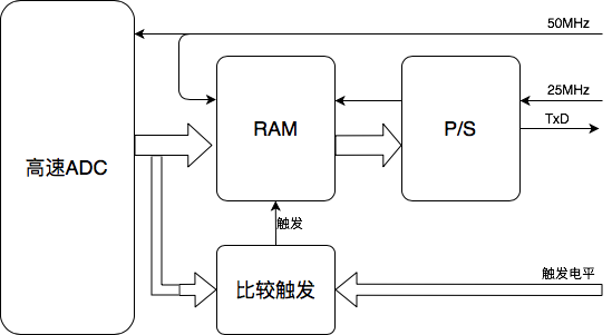
1 ADC采集数据的搬移
1.1 基于FIFO的机制
FPGA处理2个时钟域之间的数据交换:
- 一个慢的系统时钟 - 固定为25MHz
- ADC采样时钟(一般为快速时钟,比如说50MHz),它由FPGA产生并送给ADC
从ADC采集到的数据以ADC的采样频率存储到FIFO中,FIFO的数据被另一个时钟读出,并通过并/串变换发往串口(比如115200波特率)或SPI总线驱动的LCD屏幕。
假如采用的FIFO的深度为1024个字节,50MHz的采样频率,花费大约20μS的时间将FIFO填满,一旦填满,我们就不再向FIFO发送数据,存储在FIFO中的数据需要使用低速的时钟全部读出并发送出去。如果采用115200波特率的串行通信方式,大约每秒可以传送10KBytes,1024个采样点数据需要大约100ms全部发送完毕,在此期间,示波器是“盲”的,因为其采集到的数据都会被丢弃掉,不会存储到FIFO中,也就是说有99.99%的时间是“盲”的,采用这种架构带来的这种结果是非常正常的。
如果添加了“触发”的功能,则可以靠触发条件来选择数据。
ADC输出的数据总线通过8个管脚连接到FPGA,我们命名这8位的数据为“data_adc[7:0]”, 速率很高, 最好先用寄存器来同步一下:
reg [7:0] data_adc_reg;
always @(posedge clk_adc) data_adc_reg <= data_adc;
FIFO为1024个word的深度 * 8bit的宽度,50Msps的采样率,需要花费大约20μs填满FIFO。FIFO可以用FPGA内部的同步SRAM来构成,不同FPGA厂商的IP构成方式不同,但功能都是一样的。
完成了FIFO的例化以后,我们就可以通过FIFO将数据连接起来:
fifo myfifo(.data(data_adc_reg), .wrreq(wrreq), .wrclk(clk_adc), .wrfull(wrfull), .wrempty(wrempty), .q(q_fifo), .rdreq(rdreq), .rdclk(clk), .rdempty(rdempty));
向FIFO中写数据 为向FIFO中写数据,我们需要等待到空的状态,一旦FIFO的状态变“满”,则停止写数据,代码逻辑如下:
reg fillfifo;
always @(posedge clk_adc)
if(~fillfifo)
  fillfifo <= wrempty; // start when empty
else
  fillfifo <= ~wrfull; // stop when full

assign wrreq = fillfifo;
从FIFO中读取数据 只要FIFO不空,就可以从中读取数据,读出的每一个字节发送到串行输出模块
wire TxD_start = ~TxD_busy & ~rdempty;
assign rdreq = TxD_start;

async_transmitter async_txd(.clk(clk), .TxD(TxD), .TxD_start(TxD_start), .TxD_busy(TxD_busy), .TxD_data(q_fifo));
然后我们就可以通过调用“异步发送”的功能模块将数据编程变成串行,并通过“TxD”信号管脚发送出去。
完整的设计:
module oscillo(clk, TxD, clk_adc, data_adc);
input clk;
output TxD;

input clk_adc;
input [7:0] data_adc;

reg [7:0] data_adc_reg; always @(posedge clk_adc) data_adc_reg <= data_adc;

wire [7:0] q_fifo;
fifo myfifo(.data(data_adc_reg), .wrreq(wrreq), .wrclk(clk_adc), .wrfull(wrfull), .wrempty(wrempty), .q(q_fifo), .rdreq(rdreq), .rdclk(clk), .rdempty(rdempty));

// The ADC side starts filling the fifo only when it is completely empty,
// and stops when it is full, and then waits until it is completely empty again
reg fillfifo;
always @(posedge clk_adc)
if(~fillfifo)
  fillfifo <= wrempty; // start when empty
else
  fillfifo <= ~wrfull; // stop when full

assign wrreq = fillfifo;

// the manager side sends when the fifo is not empty
wire TxD_busy;
wire TxD_start = ~TxD_busy & ~rdempty;
assign rdreq = TxD_start;

async_transmitter async_txd(.clk(clk), .TxD(TxD), .TxD_start(TxD_start), .TxD_busy(TxD_busy), .TxD_data(q_fifo));

endmodule
1.2 基于双口RAM的机制
先说一下“触发” 现在,每次从串行端口接收到字符时,示波器都会被触发。 当然,这仍然不是一个非常有用的设计,但是稍后我们将对其进行改进。
我们从串行端口接收数据:
wire [7:0] RxD_data;
async_receiver async_rxd(.clk(clk), .RxD(RxD), .RxD_data_ready(RxD_data_ready), .RxD_data(RxD_data));
每次接收到新字符时,“RxDdataready”都会变高一个时钟。 我们用它来触发示波器。
再谈一下“同步”
我们需要将此“RxDdataready变高”信息从“clk”(25MHz)域传输到“clk_adc”(100MHz)域。
首先,当接收到字符时,信号“ startAcquisition”变高。
reg startAcquisition;
wire AcquisitionStarted;

always @(posedge clk)
if(~startAcquisition)
  startAcquisition <= RxD_data_ready;
else
if(AcquisitionStarted)
  startAcquisition <= 0;
我们使用2个触发器形式的同步器(将“ startAcquisition”转移到另一个时钟域)。
reg startAcquisition1; always @(posedge cll_adc) startAcquisition1 <= startAcquisition;
reg startAcquisition2; always @(posedge clk_adc) startAcquisition2 <= startAcquisition1;
最后,一旦另一个时钟域“看到”信号,它就会“回复”(使用另一个同步器“正在获取”)。
reg Acquiring;
always @(posedge clk_adc)
if(~Acquiring)
  Acquiring <= startAcquisition2;  // start acquiring?
else
if(&wraddress)  // done acquiring?
  Acquiring <= 0;

reg Acquiring1; always @(posedge clk) Acquiring1 <= Acquiring;
reg Acquiring2; always @(posedge clk) Acquiring2 <= Acquiring1;
assign AcquisitionStarted = Acquiring2;
回复将重置原始信号。
双口RAM
既然触发器可用,我们需要一个双端口RAM来存储数据,注意RAM的每一侧如何使用不同的时钟。
ram512 ram_flash(
  .data(data_flash_reg), .wraddress(wraddress), .wren(Acquiring), .wrclock(clk_flash),
  .q(ram_output), .rdaddress(rdaddress), .rden(rden), .rdclock(clk)
);
使用二进制计数器可以轻松创建ram地址总线。 首先写地址:
reg [8:0] wraddress;
always @(posedge clk_flash) if(Acquiring) wraddress <= wraddress + 1;
以及读取的地址:
reg [8:0] rdaddress;
reg Sending;
wire TxD_busy;

always @(posedge clk)
if(~Sending)
  Sending <= AcquisitionStarted;
else
if(~TxD_busy)
begin
  rdaddress <= rdaddress + 1;
  if(&rdaddress) Sending <= 0;
end
注意每个计数器如何使用不同的时钟。
最后,我们将数据发送到PC:
wire TxD_start = ~TxD_busy & Sending;
wire rden = TxD_start;

wire [7:0] ram_output;
async_transmitter async_txd(.clk(clk), .TxD(TxD), .TxD_start(TxD_start), .TxD_busy(TxD_busy), .TxD_data(ram_output));
完整的设计
module oscillo(clk, RxD, TxD, clk_adc, data_adc);
input clk;
input RxD;
output TxD;

input clk_flash;
input [7:0] data_adc;

///////////////////////////////////////////////////////////////////
wire [7:0] RxD_data;
async_receiver async_rxd(.clk(clk), .RxD(RxD), .RxD_data_ready(RxD_data_ready), .RxD_data(RxD_data));

reg startAcquisition;
wire AcquisitionStarted;

always @(posedge clk)
if(~startAcquisition)
  startAcquisition <= RxD_data_ready;
else
if(AcquisitionStarted)
  startAcquisition <= 0;

reg startAcquisition1; always @(posedge clk_adc) startAcquisition1 <= startAcquisition ;
reg startAcquisition2; always @(posedge clk_adc) startAcquisition2 <= startAcquisition1;

reg Acquiring;
always @(posedge clk_adc)
if(~Acquiring)
  Acquiring <= startAcquisition2;
else
if(&wraddress)
  Acquiring <= 0;

reg [8:0] wraddress;
always @(posedge clk_adc) if(Acquiring) wraddress <= wraddress + 1;

reg Acquiring1; always @(posedge clk) Acquiring1 <= Acquiring;
reg Acquiring2; always @(posedge clk) Acquiring2 <= Acquiring1;
assign AcquisitionStarted = Acquiring2;

reg [8:0] rdaddress;
reg Sending;
wire TxD_busy;

always @(posedge clk)
if(~Sending)
  Sending <= AcquisitionStarted;
else
if(~TxD_busy)
begin
  rdaddress <= rdaddress + 1;
  if(&rdaddress) Sending <= 0;
end

wire TxD_start = ~TxD_busy & Sending;
wire rden = TxD_start;

wire [7:0] ram_output;
async_transmitter async_txd(.clk(clk), .TxD(TxD), .TxD_start(TxD_start), .TxD_busy(TxD_busy), .TxD_data(ram_output));

///////////////////////////////////////////////////////////////////
reg [7:0] data_adc_reg; always @(posedge clk_adc) data_adc_reg <= data_adc;

ram512 ram_adc(
  .data(data_adc_reg), .wraddress(wraddress), .wren(Acquiring), .wrclock(clk_adc),
  .q(ram_output), .rdaddress(rdaddress), .rden(rden), .rdclock(clk)
);

endmodule
1.3 触发
检测一个上升沿
reg Threshold1, Threshold2;
always @(posedge clk_adc) Threshold1 <= (data_adc_reg>=8'h80);
always @(posedge clk_adc) Threshold2 <= Threshold1;

assign Trigger = Threshold1 & ~Threshold2;  // if positive edge, trigger!