过孔的使用
过孔的作用及分类
过孔的使用
在我们实际的生活中,一些简单的板子我们可以使用单层板进行绘制,但是当我们的板子变得复杂或者板子的大小固定的时候,单层板就已经不能满足我们的需求了,
此时我们需要使用双层或者四层板,这时候我们去布线的时候一条线就不会只出现在一面上,此时当我们需要让我们的走线从一面到另外一面的时候就需要过孔的存在了。
那么过孔是什么呢,顾名思义,过孔就是一个通道,它连接着顶层和底层,它的侧面覆盖着铜,金或者其他材质,这样就可以跨层进行沟通连接。
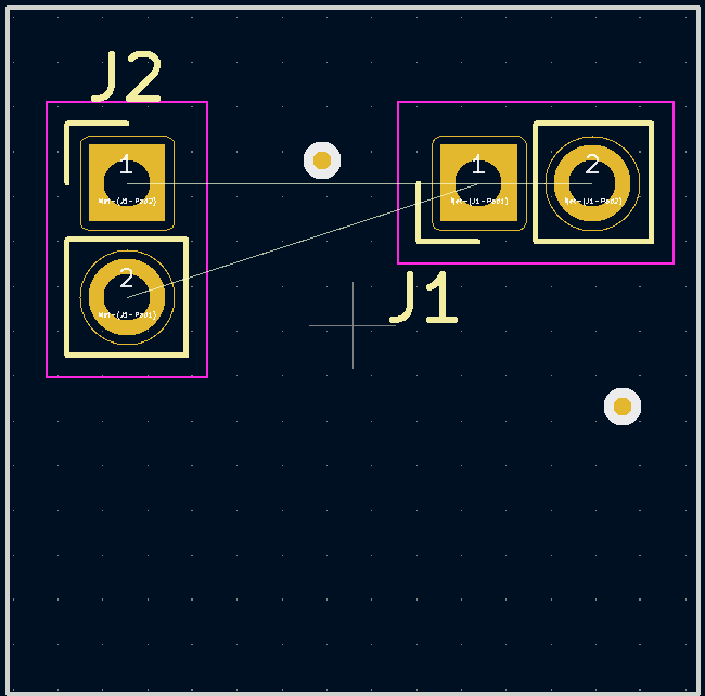
我们来简单画一个板子,并且在上面放置了过孔如图
绘制过孔
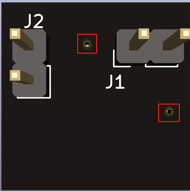
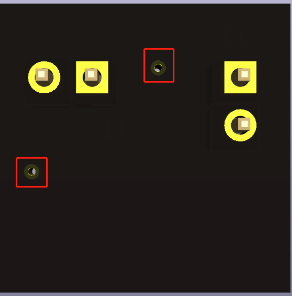
我们直接来看一下这个板子的3D效果图,如图这是正面的过孔位置
正面过孔
背面过孔
其实这个过孔和我们的插件焊盘非常的相似,只是我们的过孔没有暴露在外的铜,就是没有焊盘,所以我们不能将元器件焊接在过孔上。
过孔并不只有一种如图所示,过孔分为通孔,埋孔、盲孔、微孔:
过孔分类
下面就以四层板来简单解释一下大家再参考着图片理解一下:
1、过孔:就是从顶层一直连通底层,所有的层都是可以沟通的;
2、盲孔:盲孔就是指可以在板子的一面看到,另外一面是看不到的,就是顶层、底层连接的中间层;
3、埋孔:就是埋在里面我们在板子上是看不到的,比如四层板,埋孔就是2、3层之间的孔 ;
4、微孔:就是微通道,它常用于高密度板,之所以叫它微孔就表明它的直径是非常小的,微孔不像其他过孔一样是用机械钻头,微孔是使用激光钻孔。激光钻孔的使用可以大大缩减过孔的直径。
When you want to move a signal that travels across a trace from one side of a PCB to another (say, from front to back), you can create a via. A via is a hole with its sides covered with copper or gold (or other conductive material), that allows a trace to continue its route across layers.
In Figure 12.6, you can see the two sides of the same PCB. On the left, the arrows point to two vias in the front of the PCB, and on the right, the circles indicate the same vias on the back of the PCB. Vias are very similar to through-hole pads, except that they don’t have any exposed copper (they are covered by the solder mask), and they don’t have a pad (so you can’t solder a component). In simple circuits with only a few components, it is possible to create all of the traces on one layer of the PCB. When a PCB gets busy with more components it quickly becomes impossible to do the routing on a single layer. When multiple layers are needed, vias provide the simplest method of allowing a trace to use the available board real estate. In the Figure 12.7 you can see the types of interconnections between layers that are possible.
For through-hole components, you would design a hole that connects the top and bottom copper layers. This hole is implemented using a drill. It is wide enough to allow for the pin of the component to go through it. Vias are smaller than holes in terms of their diameter. They are not wide enough for pins to go through them, but they are plated, like holes, and they allow for electrical connection between layers to take place. A 'through via' is like a hole, but narrower. It connects the top and bottom layers. A buried via is a via that connects any two internal layers. In the fourlayer example of Figure 12.7, the buried via connects the In1.Cu and In2.Cu. A 'blind via', also connects two layers, but has one end exposed on to the outside of the board, either top or bottom. In high-density boards, another option for interconnecting layers is to use a 'micro via' (‘uvia’). A micro via is made using high-powered lasers, instead of a mechanical drill; the use of lasers makes it possible to dramatically reduce the diameter of the via.
